10.6.1. Simulator input files (Spice Opus)
The circuit we are going to simulate is a Miller OpAmp. The amplifier schematic is in file miller.sch in folder demo/design/miller/.
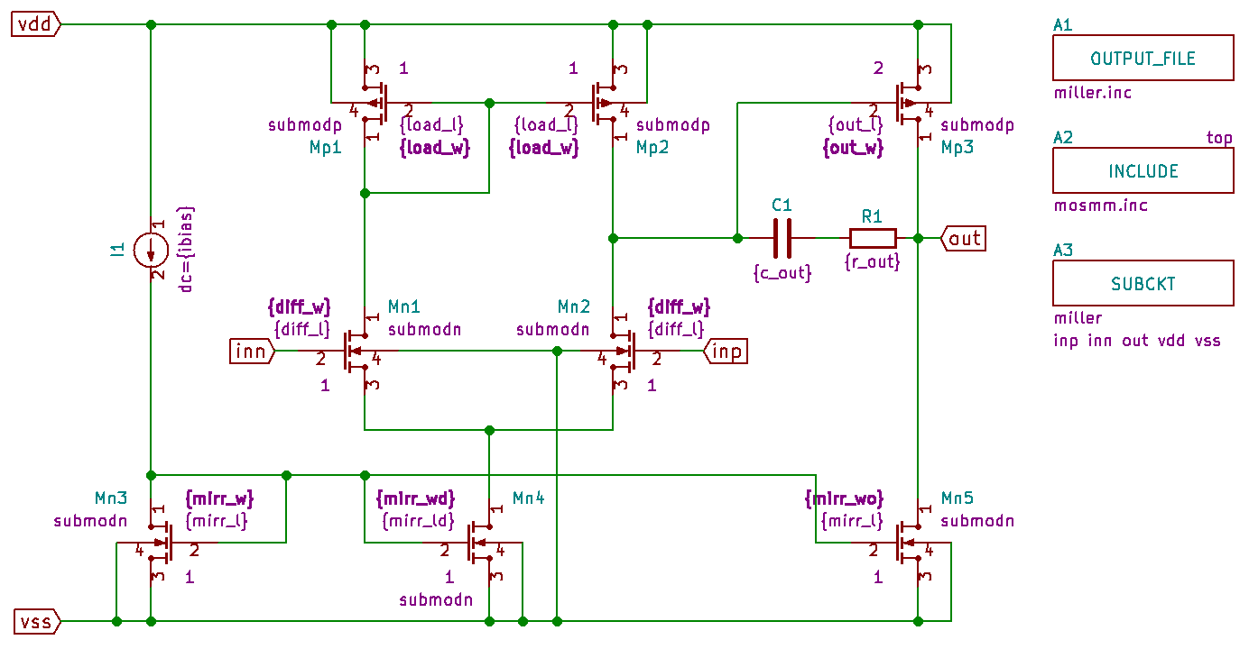
Miller OpAmp schematic.
We can see that all transistor dimensions, as well as the bias current, compensation resistor, and compensation capacitor are parameterized. We are going to use wrappers for builtin MOS devices so that we can model transistor’s mismatch parameters. The two wrappers are defined in file mosmm.inc in folder demo/design/miller/.
* Mismatch model of NMOS and PMOS, Spice Opus
*   w, l, m    ... MOS parameters
*   vtmm, u0mm ... normalized mismatch (+1 means +1 sigma)

.subckt submodn drain gate source bulk param: w l m=1 vtmm=0 u0mm=0
.param sqrtarea=sqrt(w*l*m)
.param vvt=vtmm*(5e-3*1e-6/sqrtarea/sqrt(2))
.param vu0r=u0mm*(1.04e-2*1e-6/sqrtarea/sqrt(2))
* This simple model may exhibit discontinuity or even exceed limits on channel length
*vgmm (gate gate_int) dc={vvt}
*m0 (drain gate_int source bulk) nmosmod w={w*(1+vu0r)} l={l} m={m} ad={w*0.18u} as={w*0.18u} pd={2*(w+0.18u)} ps={2*(w+0.18u)} nrs={0.18u/w} nrd={0.18u/w}
* This one is better
m0 (drain gate source bulk) nmosmod w={w} l={l} m={m} ad={w*0.18u} as={w*0.18u} pd={2*(w+0.18u)} ps={2*(w+0.18u)} nrs={0.18u/w} nrd={0.18u/w} vth0_absdelta={vvt} u0_reldelta={vu0r}
.ends

.subckt submodp drain gate source bulk param: w l m=1 vtmm=0 u0mm=0
.param sqrtarea=sqrt(w*l*m)
.param vvt=vtmm*(5.49e-3*1e-6/sqrtarea/sqrt(2))
.param vu0r=u0mm*(0.99e-2*1e-6/sqrtarea/sqrt(2))
* This simple model may exhibit discontinuity or even exceed limits on channel length
*vgmm (gate gate_int) dc={vvt}
*m0 (drain gate_int source bulk) pmosmod w={w*(1+vu0r)} l={l} m={m} ad={w*0.18u} as={w*0.18u} pd={2*(w+0.18u)} ps={2*(w+0.18u)} nrs={0.18u/w} nrd={0.18u/w}
* This one is better
m0 (drain gate source bulk) pmosmod w={w*(1+vu0r)} l={l} m={m} ad={w*0.18u} as={w*0.18u} pd={2*(w+0.18u)} ps={2*(w+0.18u)} nrs={0.18u/w} nrd={0.18u/w} vth0_absdelta={vvt} u0_reldelta={vu0r}
.ends

* cmrr 8.74552e+01 builtin BSIM3 MM model
* cmrr 8.77702e+01 subcircuit MM model
By default the netlister generates simulator’s built-in MOS devices for every
MOS symbol in the schematic. Instead we would like it to generate subcircuit
instances that use the two definitions from mosmm.inc. Beside that we want
to add two mismatch parameters to every transistor. To achieve this we customize
the netlister’s behavior with file netlister.json
in folder demo/design/miller/.
{
        "Mapping": [
		[
			null, "PMOS",
			{
				"Parameters": [ "w", "l", "m" ],
				"OutPattern": "#REF() (#PINS()) #MODEL() #PARAM() #PNV() vtmm={#REFORIG()vt} u0mm={#REFORIG()u0} #PV(Specification)",
				"SpiceDevice": "subcircuit",
				"PinMap": [ 1, 2, 3, 4 ],
				"NamePrefix": "X",
				"ValueField": null
			}
		],
		[
			null, "NMOS",
			{
				"Parameters": [ "w", "l", "m" ],
				"OutPattern": "#REF() (#PINS()) #MODEL() #PARAM() #PNV() vtmm={#REFORIG()vt} u0mm={#REFORIG()u0} #PV(Specification)",
				"SpiceDevice": "subcircuit",
				"PinMap": [ 1, 2, 3, 4 ],
				"NamePrefix": "X",
				"ValueField": null
			}
		]
	]
}
This file defines the instance name prefix to be X (NamePrefix) and
adds two parameters named vtmm and u0mm to every MOS isntance. The
values of the two parameters are specified by parameters of the form
<instance_name>vt and <instance_name>u0. If mismatch effects are
not to be simulated these two parameters should be set to their default values
(0). The actual built-in MOS instance is transistor M0 in every subcircuit
instance generated by the netlister.
After netlisting the following netlist is obtained in file miller.inc in folder demo/design/miller/.
*********
* SPICE OPUS netlister for KiCad
* (c)2017 EDA Lab FE Uni-Lj
*
* Netlister : KiCad -> Spice Opus
* Config    : /home/arpadb/pytest/demo/design/miller/netlister.json
* Source    : /home/arpadb/pytest/demo/design/miller/miller.sch
* XML input : /home/arpadb/pytest/demo/design/miller/miller.xml
* Output    : /home/arpadb/pytest/demo/design/miller/miller.inc
* Date      : Wed 31 Jul 2019 02:09:58 PM CEST
* Tool      : Eeschema 5.0.2+dfsg1-1
* Sheet 1   : / -- miller.sch
*********

.include mosmm.inc

.subckt miller inp inn out vdd vss

* Sheet: /
xmn4 (net003 net002 vss vss) submodn param: w={mirr_wd} l={mirr_ld} m=1 vtmm={mn4vt} u0mm={mn4u0}
xmn3 (net002 net002 vss vss) submodn param: w={mirr_w} l={mirr_l} m=1 vtmm={mn3vt} u0mm={mn3u0}
xmn5 (out net002 vss vss) submodn param: w={mirr_wo} l={mirr_l} m=1 vtmm={mn5vt} u0mm={mn5u0}
xmp1 (net005 net005 vdd vdd) submodp param: w={load_w} l={load_l} m=1 vtmm={mp1vt} u0mm={mp1u0}
xmp2 (net004 net005 vdd vdd) submodp param: w={load_w} l={load_l} m=1 vtmm={mp2vt} u0mm={mp2u0}
xmp3 (out net004 vdd vdd) submodp param: w={out_w} l={out_l} m=2 vtmm={mp3vt} u0mm={mp3u0}
i1 (vdd net002)  dc={ibias}
r1 (out net001) r={r_out}
c1 (net001 net004) c={c_out}
xmn1 (net005 inn net003 vss) submodn param: w={diff_w} l={diff_l} m=1 vtmm={mn1vt} u0mm={mn1u0}
xmn2 (net004 inp net003 vss) submodn param: w={diff_w} l={diff_l} m=1 vtmm={mn2vt} u0mm={mn2u0}

.ends
The top-level circuit schematic for the operating point, DC, AC, noise, and transient analysis is defined in file topdc.sch in folder demo/design/miller/.
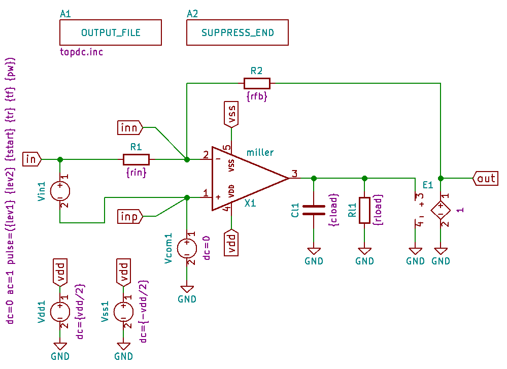
Miller Top level circuit for dc, transient, and ac analysis.
Note that we must suppress the netlister from adding .end to the netlist
because the top-level circuit will be one of the include files in the top-level
netlist. In this circuit the power supply (Vdd1), transient excitation (Vin1),
common mode source (Vcom1), feedback (R1, R2), and load (Cl1, Rl1) load are
parameterized. The amplifier output is separated from the feedback with a
voltage-controlled voltage source so that the feedback circuit does not pose
as an addittional load for the amplifier output. After netlisting the topdc.inc include file is obtained.
The top-level circuit schematic for computing rejection ratios is defined in file toprr.sch in folder demo/design/miller/.
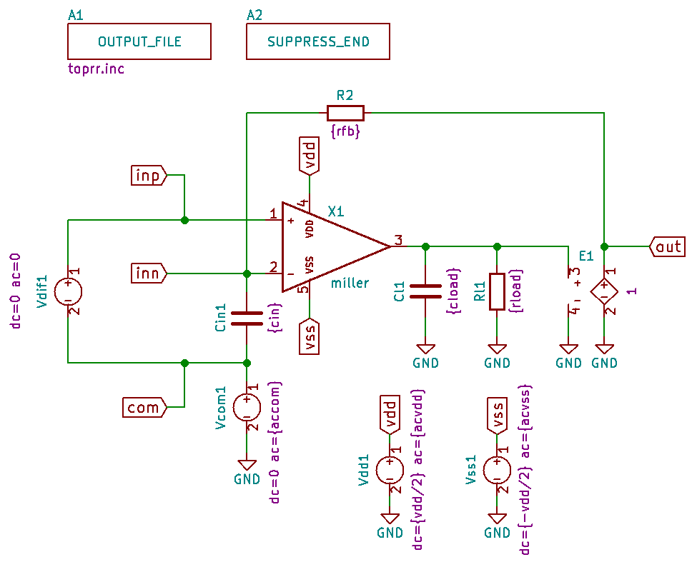
Miller Top level circuit for ac analyses on which PSRR and CMRR computations are based.
For computing the rejection ratios we must obtain the gain from the power
supplies (Vdd1, Vss1) and the common mode source (Vcom1) to the circuit’s output.
Capacitor Cin1 separates the differential excitation from shorting the DC
feedback (R2) that forces the amplifier’s operating point to be in the middle of the
active region. Its value is determined by the cin parameter which is chosen to
be large so that the effect of the separation vanishes quickly with the increasing
frequency. After netlisting the toprr.inc
include file is obtained.