The circuit
In this example the two-stage operational amplifier will be optimised by optimize command. The circuit is shown in figure below. It consists of two stages, the first of which is a differential stage with p-channel MOSFETs m1 and m2 and the current mirror m3 and m4 acting as an active load. The second stage is a simple CMOS inverter with m6 as driver and m5 acting as an active load. The output of the second stage is connected to its input by compensation capacitance cc. The configuration below is made in an n-well CMOS process.
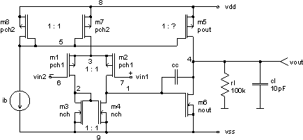
The operational amplifier is biased by an independent current source ib. Transistors m7 and m8 have equal sizes. Thus, current ib also flows in the differential input stage. Transistor m5 is expected to be much larger. Thus, the current in the second stage is expected to be much larger, as well.
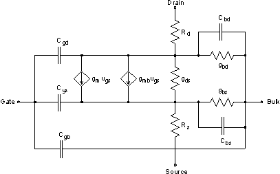
For small signals (ac analysis) SPICE replaces each MOS transistor with equivalent circuit below.
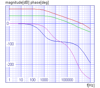
The analysis of the operational amplifier for small signals gives us quite complicated expression of transfer function Au(jw) in s = jw plane. But we can obtain a simplified expression, which is valid only for relatively low frequencies.
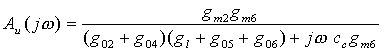
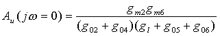
We can see that the gain of the amplifier is approximately given by:
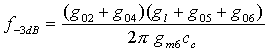
And the first (dominant) pole of the amplifier is at frequency:
In equations above the transistor transconductance gm represents gm + gmb in SPICE small signal equivalent circuit, and g0 represents gds + gbd.
The optimisation parameters are channel lengths and widths off all transistors and compensation capacitance cc. This way we get 17 dimensional optimisation problem, but because the pairs of transistors m1 and m2, m3 and m4, and m7 and m8 are the same we have 11 dimensional optimisation problem. We can also determine the explicit constraints of optimisation parameters. For 3mm CMOS n-well technology we determine that:
4mm < channel width <
200mm
4mm < channel length <
40mm
1fF <
cc < 5pF
All transistors are supposed to operate in saturation region, thus all drain-source voltages have to be high enough
v(1) > -1.38V
v(3) > 1.23V
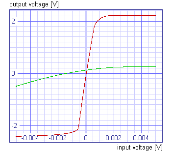
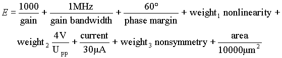
We want to design the CMOS operational amplifier, which will have high gain, high bandwidth (f-3dB), high phase margin, small current consumption, small nonlinearity, high peak-to-peak output voltage, small offset voltage and which will take small area. All those requirements are gathered in cost function, which is defined by:
We change w and l parameters of transistors m1, m3, m5, m6 and m7 in every iteration of optimisation process. The w and l parameters of transistors m2, m4 and m8 are changed as well and are equal to w and l parameters of transistors m1, m3 and m7. We also have to change source and drain areas and perimeters of all transistors. SPICE mos model parameter lambda is changed as well, because it depends on channel length. For all details see file cmos_operational_amplifier.cir. The CMOS operational amplifier was optimised by Hooke-Jeeves's optimisation method.
We can get values of gm and g0 for all transistors by show command. For optimised circuit we get:
|
gm2 =
9.28mS
gm6 = 247mS g02 = 11.9nS g04 = 22.3nS g05 = 958nS g06 = 2.07mS gl = 10mS cc = 504fF |
| calculated | SPICE OPUS | |
| Au(jw = 0) | 74.2dB | 70.7dB |
| f-3dB | 569Hz | 601Hz |
Optimised CMOS operational amplifier has:
|
gain = 70.7dB
bandwidth = 601Hz phase margin = 51.3° peak to peak voltage = 3.66V current consumption = 43.8mA area = 4407mm2 |