10.5.1. Using the pyopus.lib library in eeschema
For drawing schematics that will be used for generating netlists you can use arbitrary KiCad schematic components. But the most straightforward way is to use the pyopus.lib library of schematic components. Predefined rules exist for netlisting these components. For other KiCad schematic components you will have to write your own netlisting rules. In some cases even the default netlisting rule will be good enough.
One KiCad schematic can be subdivied in several .sch files, but in the end this hierarchy will be flattened to produce one netlist file which is either a top-level netlist or defines one subcircuit.
First you should copy the pyopus.lib and pyopus.dcm files to the
folder where your schematic files will be stored. To introduce the PyOPUS
netlister for KiCad we are going to draw two schematics. The first one
(miller.sch) defines a Miller operational transconductance amplifier (OTA)
as a subcircuit. The second one (topdc.sch) uses this subcircuit and
simulates its DC and AC behavior.
In the folder where the schematic files will be stored start eeschema to
create miller.sch by typing
eeschema miller.sch
Now you must add pyopus.lib to the list of libraries, In the main menu choose Preferences/Component Libraries. In the window that pops up click on the Add button. Browse to the folder with your schematic project and select pyopus.lib. Confirm selection and ckick OK.
Under Windows first start eeschema and select File/Save Current Sheet As in the menu. Save the empty sheet in the folder where you put the pyopus.lib and pyopus.dcm files. After that you can proceed with adding pyopus.lib to the list fo libraries.
The Miller OTA schematic is constructed using the following components from pyopus.lib
- NMOS and PMOS for the MOS transistors
- RES and CAP for the resistor and capacitor
- ISRC for the independent current source
- OUTPUT_FILE for defining the output netlist file name
- SUBCKT for defining the subciruit name and pin order
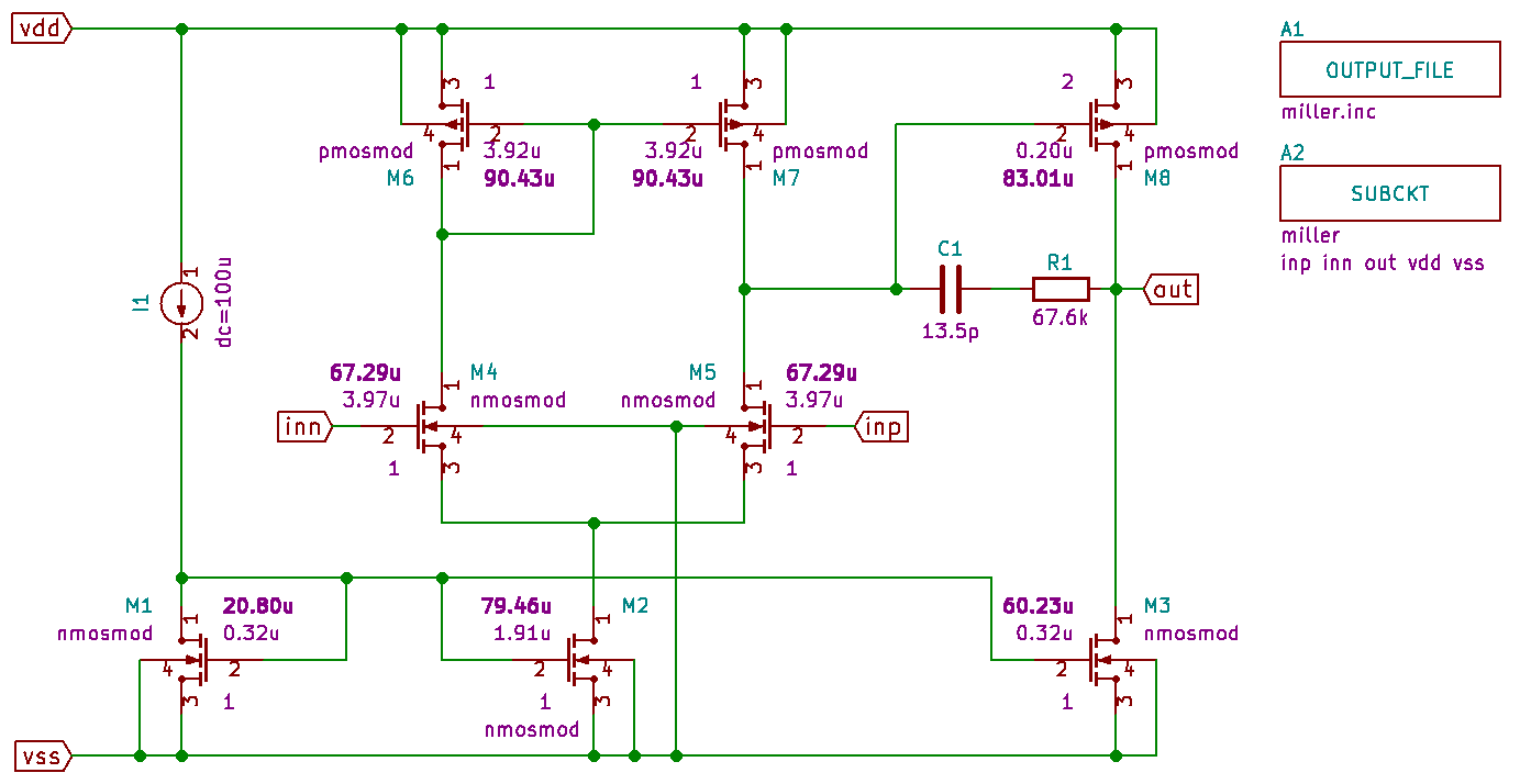
Miller OpAmp schematic.
Note that at netlisting KiCad will insist that all your component names end with a number. So don’t waste your time trying to force Ma as the MOS transistor name. Name it Ma1 instead.
MOS transistors have 3 numbers associated with every symbol. The bold one is the channel width (W). Right above/below it (depending on symbol’s rotation) is the channel length (L). Somewhat further away is the multiplier factor (M). The model name is specified as the Model filed.
By default the netlister will recognize components GND, GNDA, GNDD, GNDPWR, and
GNDREF as ground nodes. You can change this in the netlister configuration. See
the documentation of pyopus.netlister on how to do this. The customized
configuration must be stored in a netlister.json file in the folder where
the intermediate XML netlists will be generated by KiCad.
The pins of the subcircuit must be named with global labels. If you place a SUBCKT component from pyopus.lib the whole schematic will be treated as a subcircuit definition. The name of the subcircuit and the net names of its pins are defined as Fields of the SUBCKT component.
To define subcircuit parameters use the SUBCKT_PARAM components (one for
every parameter). Arbitrary parameters can be defined using the PARAM
component (one per parameter). Every PARAM component translated to one
.param statement inside the subcircuit definition (or in the top-level
netlist of the schematic defines a top-level netlist).
To generate the netlist you must first add the netlister plugin to KiCad.
The instructions for this are availabel in the documentation of
pyopus.netlister.kicad. This needs to be done only once. KiCad will
remember your plugin’s settings even after you close eeschema.
Select Tools/Generate Netlist File in the eeschema menu. A window will pup
up. Select the Spice Opus tab and click on the Generate button. A file dialog
will pup up asking you for the netlist file name, After entering it and
clicking the Save button the intermediate XML netlist will be generated
and the PyOPUS KiCad netlister plugin will be invoked. This plugin reads
the XML file and the netlister configuration files (.json files) that
customize its behavior. After that it outputs the nelist. If you place an
OUTPUT_FILE component in your schematic this component will define the name
of the netlist file regardless of what you specify in the file dialog (the
file name will only be used for the intermediate netlist). After the netlist
file is generated a window will pop up showing the contents of the netlist
file miller.inc.
*********
* SPICE OPUS netlister for KiCad
* (c)2017 EDA Lab FE Uni-Lj
*
* Netlister : KiCad -> Spice Opus
* Config    : default used
* Source    : /home/arpadb/pytest/demo/kicad/01-schem/miller.sch
* XML input : /home/arpadb/pytest/demo/kicad/01-schem/miller.xml
* Output    : /home/arpadb/pytest/demo/kicad/01-schem/miller.inc
* Date      : Thu 09 Nov 2017 05:58:57 PM CET
* Tool      : Eeschema 4.0.5+dfsg1-4
* Sheet 1   : / -- miller.sch
*********

.subckt miller inp inn out vdd vss

* Sheet: /
m2 (net004 net002 vss vss) nmosmod w=79.46u l=1.91u m=1
m1 (net002 net002 vss vss) nmosmod w=20.80u l=0.32u m=1
m3 (out net002 vss vss) nmosmod w=60.23u l=0.32u m=1
m6 (net005 net005 vdd vdd) pmosmod w=90.43u l=3.92u m=1
m7 (net003 net005 vdd vdd) pmosmod w=90.43u l=3.92u m=1
m8 (out net003 vdd vdd) pmosmod w=83.01u l=0.20u m=2
i1 (vdd net002)  dc=100u
r1 (out net001) r=67.6k
c1 (net001 net003) c=13.5p
m4 (net005 inn net004 vss) nmosmod w=67.29u l=3.97u m=1
m5 (net003 inp net004 vss) nmosmod w=67.29u l=3.97u m=1

.ends
You can close it by pressing Enter or Esc or clicking on the Close
button.
To define the top-level netlist start another instance of eeschema by typing
eeschema topdc.sch
Note eeschema will complaint that it is already running. Simply ignore the message and click Yes top continue. Add pyopus.lib to the list of libraries. The top level schematic uses the following pyopus.lib components
- VSRC for the independent voltage sources
- VCVS for the voltage-controlled voltage source
- RES and CAP for resistors and capacitors
- OPAMP for the opamp
- OUTPUT_FILE for specifying the output netlist file name
- INCLUDE for including an external file (
miller.inc) - LIB for including section
tmof the library file (cmos180n.lib)
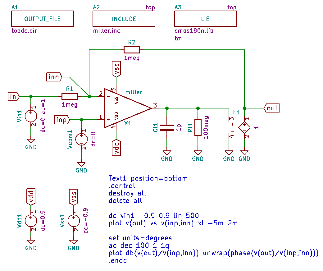
Testbench circuit schematic.
All nodes that will be accessed by the Spice Opus commands are named
explicitly with global labels. The Value filed of the OPAMP is set to the
name of the subcircuit that defines the Miller OTA (included from file
miller.inc). By default all components that do not have a netlisting
rule defined are netlisted as subcircuits. The Value field specifies the
subcircuit name. The nodes of the subcircuit instance are dumped in the
increasing pin number order of the component.
Any text block will be added to the netlist above/below netlisted components if it starts with the line
Text<number> position=top|bottom
If there are multiple text blocks they are dumped in in the increasing
number order. Note that the schematic file must be saved before netlisting
so that the netlister can extract the text blocks from the schematic file.
We use this text block feature to add a .control block to the netlist
with the commands thet will run a DC and an AC analysis and plot the results.
After netlisting the topdc.sch file the following netlist will be written
to the topdc.cir file (due to the OUTPUT_FILE component).
*********
* SPICE OPUS netlister for KiCad
* (c)2017 EDA Lab FE Uni-Lj
*
* Netlister : KiCad -> Spice Opus
* Config    : default used
* Source    : /home/arpadb/pytest/demo/kicad/01-schem/topdc.sch
* XML input : /home/arpadb/pytest/demo/kicad/01-schem/topdc.xml
* Output    : /home/arpadb/pytest/demo/kicad/01-schem/topdc.cir
* Date      : Thu 09 Nov 2017 05:59:20 PM CET
* Tool      : Eeschema 4.0.5+dfsg1-4
* Sheet 1   : / -- topdc.sch
*********

.include miller.inc
.lib 'cmos180n.lib' tm


* Sheet: /
x1 (inp inn net001 vdd vss) miller
vdd1 (vdd 0)  dc=0.9
r2 (out inn) r=1meg
r1 (inn in) r=1meg
vcom1 (inp 0)  dc=0
vin1 (in 0)  dc=0 ac=1
vss1 (vss 0)  dc=-0.9
cl1 (net001 0) c=1p
e1 (out 0 net001 0) gain=1
rl1 (net001 0) r=100meg

* Verbatim block Text1 from sheet /
.control
destroy all
delete all

dc vin1 -0.9 0.9 lin 500
plot v(out) vs v(inp,inn) xl -5m 2m

set units=degrees
ac dec 100 1 1g
plot db(v(out)/v(inp,inn)) unwrap(phase(v(out)/v(inp,inn)))
.endc

.end
You can run the simulation by typing
spiceopus topdc.cir
Demo files for this section can be found here.